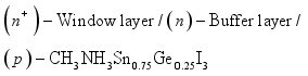
In this work, we have carried out a study in the modeling of photovoltaic devices based on lead-free perovskite materials, such as CH3NH3Sn(1-y)GeyI3, in which the germanium content varies from 0 to 1, using thin ZnO, TiO2 or SnO2, films as window layers. Thin Cu2O or NiO layers used as buffer layers ensure the n-p junction with the perovskite absorber material and act as an interface layer with the transport window layer. With the above window and buffer layer materials, photovoltaic devices have been designed. The study highlights the influence of geometric parameters such as the diffusion length of the minority carriers in the buffer layer as well as the thickness of this layer on the performance of photovoltaic devices. The evolution of the internal quantum efficiency is analyzed as a function of the window and buffer layer materials and also as a function of various other parameters including the thickness of the buffer layer materials and the minority carrier diffusion length in these materials. The results showed that NiO thin films offer better performances, especially when combined with ZnO or SnO2 window layers, respectively. The corresponding models with structures ZnO(n+)/NiO(n)/CH3NH3Sn0.75Ge0.25I3(p) and SnO2(n+)/NiO(n)/CH3NH3Sn0.75Ge0.25I3(p) give an internal quantum efficiency of 72.7% and 70.9% respectively.
| Published in | Advances in Materials (Volume 14, Issue 4) |
| DOI | 10.11648/j.am.20251405.12 |
| Page(s) | 95-104 |
| Creative Commons |
This is an Open Access article, distributed under the terms of the Creative Commons Attribution 4.0 International License (http://creativecommons.org/licenses/by/4.0/), which permits unrestricted use, distribution and reproduction in any medium or format, provided the original work is properly cited. |
| Copyright |
Copyright © The Author(s), 2025. Published by Science Publishing Group |
Perovskites, Modeling, Lead-free Perovskite Solar Cell
 material. With the above window and buffer layer materials, the following photovoltaic devices ZnO(n+)/Cu2O(n)/CH3NH3Sn0.75Ge0.25I3(p), TiO2(n+)/Cu2O(n)/CH3NH3Sn0.75Ge0.25I3(p), SnO2(n+)/Cu2O(n)/CH3NH3Sn0.75Ge0.25I3(p) and ZnO(n+)/NiO(n)/CH3NH3Sn0.75Ge0.25I3(p), TiO2(n+)/NiO(n)/CH3NH3Sn0.75Ge0.25I3(p), SnO2(n+)/NiO(n)/CH3NH3Sn0.75Ge0.25I3(p) have been designed. In a recent work, the influence of window layers on the spectral evolution of the total current flowing through such solar cells, have been investigated
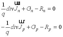
 . The absorber layer is the CH3NH3Sn0.75Ge0.25I3 perovskite. It is a p-type semiconductor material and has a function of absorbing incident photons from solar radiation to generate electron-hole pairs
 and 2.0 eV for
 , which influences the optoelectronic properties of the solar cell. By enhancing the germanium content, we can thus continuously vary the band gap width between 1.3 eV and 2.0 eV and obtain different solar cells
  . The window layer allows incident photons to pass through to the absorber, and also collects charge thanks to its high conductivity.
 and
and 
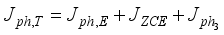
 is the minority carries concentration,
  are the hole diffusion length and the hole diffusion coefficient in the windows layer region, respectively.
  and
and  represent the hole lifetime and absorption coefficient of the windows layer respectively.
  is the reflection coefficient and
  is incident photon flux of energy E and wavelength
  .
. 
 is the recombination velocity on the front surface of the window layer.
  in this region is given by:
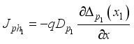
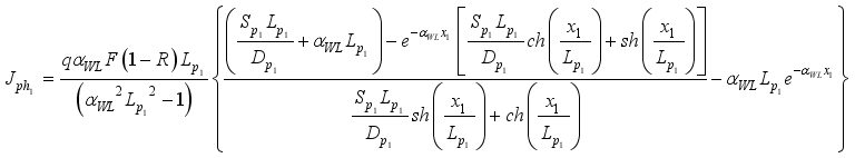
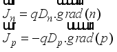
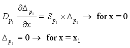
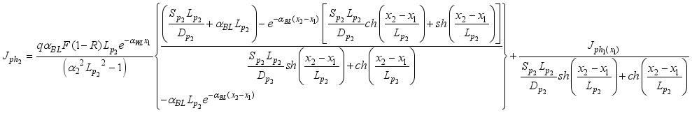
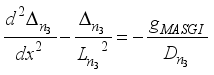
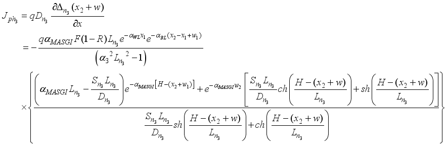
 serving as a buffer layer, the minority carriers are the holes. The continuity equation for the minority carriers is given by:
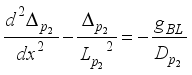
 and
and 
 .
.  is the minority carries concentration.
  are the hole diffusion length and the hole diffusion coefficient in the buffer layer region, respectively.
  and
and  represent the hole lifetime and absorption coefficient of the buffer layer respectively.
 region is given by:

 and
and 
 is the minority carries concentration.
  are the electron diffusion length and the electron diffusion coefficient in the absorber layer region, respectively.
  represent the electron lifetime and
  the absorption coefficient of the absorber CH3NH3Sn0.75Ge0.25I3 layer.
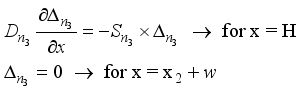
 while its thickness values are varied from
  . The hole diffusion length and the ZnO window layer thickness are set at
  , respectively. The electron diffusion length in the CH3NH3Sn0.75Ge0.25I3 absorber layer is set at to
  and its thickness at
  .
.  . The diffusion length of the holes varies from
  .
.  , and the thickness values range from
  . The hole diffusion length and thickness of the TiO2 window layer is
  respectively. The electron scattering length of the CH3NH3Sn0.75Ge0.25I3 absorber layer is estimated at and its thickness at
  .
.  . The thickness of the Cu2O layer is fixed at
  .
.  , the internal quantum efficiency is between 50% and 60%. For thicknesses in the range, the overall internal quantum efficiency remains low for values between 40% and 50%. These low internal quantum efficiency values can be explained by the fact that when the layer thickness is large relative to the diffusion length, the majority of photogenerated carriers in this region do not reach the junction to contribute to the current delivered by the solar cell. These are absorbed by the (in the energy range above 2.1 eV) or recombine.
  . The hole diffusion length and thickness of the ZnO window layer is
 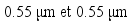 respectively. The electron scattering length of the CH3NH3Sn0.75Ge0.25I3 absorber layer is estimated at
  and its thickness at
  .
.  . The diffusion lengths of the holes vary from
  .
.  , the internal quantum efficiency is between 60% and 80%. Those in the
 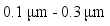 range give the best performance. Internal quantum efficiency drops from 70.2% to 64.3% for thicknesses between
 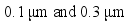 . This is because, for each given thickness, there is a diffusion length at which the internal quantum efficiency is maximum.
  . The NiO buffer layer, also acts as a window, enabling the electrical transition between the and the absorber material
  . The absorption coefficients values of the NiO layer were taken from
 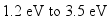 .
.  . We vary the thickness from
  . The carrier scattering length in the ZnO layer and its thickness are evaluated at 0.55 micrometers. For the perovskite layer, its thickness is set at
  and the diffusion length of its carriers at
  .
.  . The diffusion length varies from
  . The carrier diffusion length in the ZnO layer and its thickness are evaluated at
  . For the perovskite layer, its thickness is set at
  and the diffusion length of its carriers at
  .
.  , the internal quantum efficiency is between 70% and 80%. Those in the
  range give the best performance. Internal quantum efficiency drops from 70.2% to 64.3% for thicknesses between
  . This is because, for each given thickness, there is a scattering length at which the internal quantum efficiency is maximum.
  . We vary the thickness from
  . The carrier diffusion length in the ZnO layer and its thickness are evaluated at
  . For the perovskite layer, its thickness is set at
  and the diffusion length of its carriers at
  .
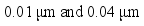
.  , and the diffusion length varies from 0.01 to 0.3 mm. The diffusion length of the carriers in the ZnO layer and its thickness are evaluated at 0.55 mm. For the perovskite layer, its thickness is set at 0.5 mm and the diffusion length of its carriers at 0.5 mm.
  and the thickness varies from
  .
.  and the diffusion length varies from
  . The thickness and diffusion length of the SnO2 carriers are estimated at
  . The perovskite layer thickness is set at
  and the carrier diffusion length at
  .
.  , the internal quantum efficiency is between 70% and 80%. Those in the
  range give the best performance. Internal quantum efficiency drops from 68.1% to 62.7% for thicknesses between
  . This is because, for each given thickness, there is a scattering length at which the internal quantum efficiency is at its maximum.
  , and the carrier scattering lengths at
  . The values for carrier scattering lengths and NiO layer thicknesses are
  respectively. For the
 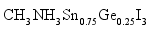 absorber layer, the carrier diffusion length is equal to
  and the thickness
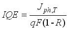
  . For the three different models ZnO(n+)/NiO(n)/CH3NH3Sn0.75Ge0.25I3(p), TiO2(n+)/NiO(n)/CH3NH3Sn0.75Ge0.25I3(p) and SnO2(n+)/NiO(n)/CH3NH3Sn0.75Ge0.25I3(p) and the internal quantum efficiency are 72.7%, 50.9% and 70.9% respectively. The ZnO and NiO materials for transport layers with the structure ZnO(n+)/NiO(n)/CH3NH3Sn0.75Ge0.25I3(p) model give the best internal quantum efficiency of 72.7%.
  . The corresponding model with structure ZnO(n+)/NiO(n)/CH3NH3Sn0.75Ge0.25I3(p) gives an internal quantum efficiency of 72.7%.
 IQE | Internal Quantum Efficiency |
Ge | Germanium |
Sn | Tin |
WL | Windows Layer |
BL | Buffer Layer |
| [1] | A. Kojima, K. Teshima, Y. Shirai, T. Miyasaka, Organometal halide perovskites as visible-light sensitizers for photovoltaic cells J. Am. Chem. Soc. 131 (2009) 6050. |
| [2] | Y. C. Zhao, W. K. Zhou, X. Zhou, K. H. Liu, D. P. Yu, Q. Zhao, Quantification of light-enhanced ionic transport in lead iodide perovskite thin films and its solar cell applications Light: Sci. Appl., 6 (2017) 6243. |
| [3] | W. J. Yin, T. Shi, Y. Yan, Unique properties of halide perovskites as possible origins of the superior solar cell performance, Adv. Mater., 26 (2014) 4653. |
| [4] | J. Jiang, Q. Wang, Z. Jin, X. Zhang, J. Lei, H. Bin, Z. G. Zhang, Y. Li, S. Liu, Polymer doping for high-efficiency perovskite solar cells with improved moisture stability, Adv. Energy Mater. 8 (2018) 1701757. |
| [5] | M. H. Kumar, S. Dharani, W. L. Leong, P. P. Boix, R. R. Prabhakar, T. Baikie, C. Shi, H. Ding, R. Ramesh, M. Asta, M. Graetzel, S. G. Mhaisalkar, N. Mathews, Lead‐free halide perovskite solar cells with high photocurrents realized through vacancy modulation, Adv. Mater., 26 (2014) 7122. |
| [6] | D. H. Cao, C. C. Stoumpos, T. Yokoyama, J. L. Logsdon, T. B. Song, O. K. Farha, M. R. Wasielewski, J. T. Hupp, M. G. Kanatzidis, Thin Films and Solar Cells Based on Semiconducting Two-Dimensional Ruddlesden–Popper (CH3(CH2)3NH3)2(CH3NH3)n−1SnnI3n+1 Perovskites, ACS Energy Lett., 2 (2017) 982. |
| [7] | B. W. Park, B. Philippe, X. Zhang, H. Rensmo, G. Boschloo, E. M. J. Johansson, Bismuth Based Hybrid Perovskites A3Bi2I9 (A: Methylammonium or Cesium) for Solar Cell Application, Adv. Mater., 27 (2015) 6806. |
| [8] | K. Eckhardt, V. Bon, J. Getzschmann, J. Grothe, F. M. Wisser, S. Kaskel, Crystallographic insights into (CH3NH3)3(Bi2I9): a new lead-free hybrid organic–inorganic material as a potential absorber for photovoltaics, Chem. Commun., 52 (2016) 3058. |
| [9] | M. Jahandar, J. H. Heo, C. E. Song, K.-J. Kong, W. S. Shin, J. C. Lee, S. H. Im, S. J. Moon, Highly efficient metal halide substituted CH3NH3I(PbI2)1−X(CuBr2)X planar perovskite solar cells, Nano Energy 27 (2016) 330. |
| [10] | T. Krishnamoorthy, H. Ding, C. Yan, W. L. Leong, T. Baikie, Z. Zhang, M. Sherburne, S. Li, M. Asta, N. Mathews, S. G. Mhaisalkar, Lead-free germanium iodide perovskite materials for photovoltaic application, J. Mater. Chem. 3 (2015) 23829. |
| [11] | K. M. Boopathi, P. Karuppuswamy, A. Singh, C. Hanmandlu, L. Lin, S. A. Abbas, C. C. Chang, P. C. Wang, G. Li, C. W. Chu, Solution-processable antimony-based light-absorbing materials beyond lead halide perovskites, J. Mater. Chem., 5 (2017) 20843. |
| [12] | C. Zuo, L. Ding, Angew. Lead-free Perovskite Materials (NH4)3Sb2IxBr9−x, Chem., 56 (2017) 6528. |
| [13] | L. Zhang, W. Liang, How the structures and properties of two-dimensional layered perovskites MAPbI3 and CsPbI3 vary with the number of layers, J. Phys. Chem. Lett., 8 (2017) 1517-1523. |
| [14] | M. Kar, R. Sarkar, S. Pal, P. Sarkar, Lead Free Two-Dimensional Mixed Tin and Germanium Halide Perovskites for Photovoltaic Applications, J. Phys. Chem., 125 (2021) 74−81. |
| [15] | S. Nagane, D. Ghosh, R. L. Z. Hoye, B. Zhao, S. Ahmad, A. B. Walker, M. S. Islam, S. Ogale, A. Sadhanala, Lead-free perovskite semiconductors based on germanium-tin solid solutions: Structural and optoelectronic properties, J. Phys. Chem. C, 122 (2018) 5940−5947. |
| [16] | N. F. A. Shammary, Optical characteristics of NiO thin film on glass formed by chemical spray pyrolysis. Journal of kufa-Physics, 2 (2010). |
| [17] | S. Seck, A. Sow, M. S. Mané, A. Ndiaye, E. M. Keita, B. Ndiaye, B. Mbow, and C. Sène, Modeling and Analysis of a Mixed Sn-Ge Lead Free Perovskite Based Solar Cells, American Journal of Energy Research, (12) 1 (2024) 1-7. |
| [18] | S. Seck, A. Sow, M. S. Mane, M. Faye, E. H. M. Keita, A. Ndiaye, B. Ndiaye, B. Mbow, C. Sene, Influence of Window Layers on the Spectral Evolution of the Total Current Flowing Through a Solar Cell Based on Lead-Free Perovskite Materials, International Journal of Materials Science and Applications, (3) 14 (2025) 79-88. |
APA Style
Seck, S., Sow, A., Mane, M. S., Faye, M., Keita, E. H. M., et al. (2025). Investigation on Buffer Layers Influence on the Internal Quantum Efficiency of CH3NH3Sn(1-y)GeyI3 Lead-Free Perovskite-Based Solar Cells. Advances in Materials, 14(4), 95-104. https://doi.org/10.11648/j.am.20251405.12
ACS Style
Seck, S.; Sow, A.; Mane, M. S.; Faye, M.; Keita, E. H. M., et al. Investigation on Buffer Layers Influence on the Internal Quantum Efficiency of CH3NH3Sn(1-y)GeyI3 Lead-Free Perovskite-Based Solar Cells. Adv. Mater. 2025, 14(4), 95-104. doi: 10.11648/j.am.20251405.12
AMA Style
Seck S, Sow A, Mane MS, Faye M, Keita EHM, et al. Investigation on Buffer Layers Influence on the Internal Quantum Efficiency of CH3NH3Sn(1-y)GeyI3 Lead-Free Perovskite-Based Solar Cells. Adv Mater. 2025;14(4):95-104. doi: 10.11648/j.am.20251405.12
@article{10.11648/j.am.20251405.12,
  author = {Saliou Seck and Alioune Sow and Mamadou Salif Mane and Modou Faye and El Hadji Mamadou Keita and Amadou Ndiaye and Bachirou Ndiaye and Babacar Mbow and Cheikh Sene},
  title = {Investigation on Buffer Layers Influence on the Internal Quantum Efficiency of CH3NH3Sn(1-y)GeyI3 Lead-Free Perovskite-Based Solar Cells
},
  journal = {Advances in Materials},
  volume = {14},
  number = {4},
  pages = {95-104},
  doi = {10.11648/j.am.20251405.12},
  url = {https://doi.org/10.11648/j.am.20251405.12},
  eprint = {https://article.sciencepublishinggroup.com/pdf/10.11648.j.am.20251405.12},
  abstract = {In this work, we have carried out a study in the modeling of photovoltaic devices based on lead-free perovskite materials, such as CH3NH3Sn(1-y)GeyI3, in which the germanium content varies from 0 to 1, using thin ZnO, TiO2 or SnO2, films as window layers. Thin Cu2O or NiO layers used as buffer layers ensure the n-p junction with the perovskite absorber material and act as an interface layer with the transport window layer. With the above window and buffer layer materials, photovoltaic devices have been designed. The study highlights the influence of geometric parameters such as the diffusion length of the minority carriers in the buffer layer as well as the thickness of this layer on the performance of photovoltaic devices. The evolution of the internal quantum efficiency is analyzed as a function of the window and buffer layer materials and also as a function of various other parameters including the thickness of the buffer layer materials and the minority carrier diffusion length in these materials. The results showed that NiO thin films offer better performances, especially when combined with ZnO or SnO2 window layers, respectively. The corresponding models with structures ZnO(n+)/NiO(n)/CH3NH3Sn0.75Ge0.25I3(p) and SnO2(n+)/NiO(n)/CH3NH3Sn0.75Ge0.25I3(p) give an internal quantum efficiency of 72.7% and 70.9% respectively.
},
 year = {2025}
}
TY  - JOUR
T1  - Investigation on Buffer Layers Influence on the Internal Quantum Efficiency of CH3NH3Sn(1-y)GeyI3 Lead-Free Perovskite-Based Solar Cells

AU  - Saliou Seck
AU  - Alioune Sow
AU  - Mamadou Salif Mane
AU  - Modou Faye
AU  - El Hadji Mamadou Keita
AU  - Amadou Ndiaye
AU  - Bachirou Ndiaye
AU  - Babacar Mbow
AU  - Cheikh Sene
Y1  - 2025/10/31
PY  - 2025
N1  - https://doi.org/10.11648/j.am.20251405.12
DO  - 10.11648/j.am.20251405.12
T2  - Advances in Materials
JF  - Advances in Materials
JO  - Advances in Materials
SP  - 95
EP  - 104
PB  - Science Publishing Group
SN  - 2327-252X
UR  - https://doi.org/10.11648/j.am.20251405.12
AB  - In this work, we have carried out a study in the modeling of photovoltaic devices based on lead-free perovskite materials, such as CH3NH3Sn(1-y)GeyI3, in which the germanium content varies from 0 to 1, using thin ZnO, TiO2 or SnO2, films as window layers. Thin Cu2O or NiO layers used as buffer layers ensure the n-p junction with the perovskite absorber material and act as an interface layer with the transport window layer. With the above window and buffer layer materials, photovoltaic devices have been designed. The study highlights the influence of geometric parameters such as the diffusion length of the minority carriers in the buffer layer as well as the thickness of this layer on the performance of photovoltaic devices. The evolution of the internal quantum efficiency is analyzed as a function of the window and buffer layer materials and also as a function of various other parameters including the thickness of the buffer layer materials and the minority carrier diffusion length in these materials. The results showed that NiO thin films offer better performances, especially when combined with ZnO or SnO2 window layers, respectively. The corresponding models with structures ZnO(n+)/NiO(n)/CH3NH3Sn0.75Ge0.25I3(p) and SnO2(n+)/NiO(n)/CH3NH3Sn0.75Ge0.25I3(p) give an internal quantum efficiency of 72.7% and 70.9% respectively.

VL  - 14
IS  - 4
ER  -
Department of Physics, Cheikh Anta Diop University, Dakar, Senegal
Department of Physics, Cheikh Anta Diop University, Dakar, Senegal
Department of Physics, Cheikh Anta Diop University, Dakar, Senegal
Department of Physics, Cheikh Anta Diop University, Dakar, Senegal
Department of Physics, Cheikh Anta Diop University, Dakar, Senegal
Department of Physics, Cheikh Anta Diop University, Dakar, Senegal
Department of Physics, Cheikh Anta Diop University, Dakar, Senegal
Department of Physics, Cheikh Anta Diop University, Dakar, Senegal
Department of Physics, Cheikh Anta Diop University, Dakar, Senegal
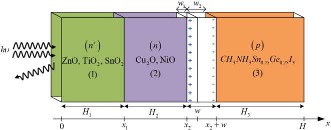
Figure 1. CH3NH3Sn0.75Ge0.25I3(p) perovskite solar cell Model.
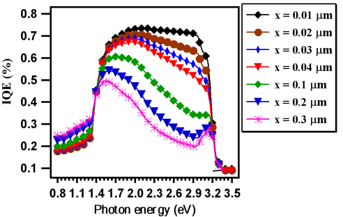
Figure 2. Influence of the Cu2O layer thickness on the internal quantum efficiency: case of the solar cell with ZnO window layer.
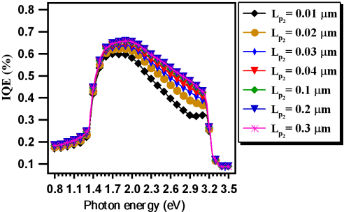
Figure 3. Evolution of the internal quantum efficiency with the minority carrier diffusion length in the Cu2O buffer layer: case of the solar cell with the ZnO window layer.
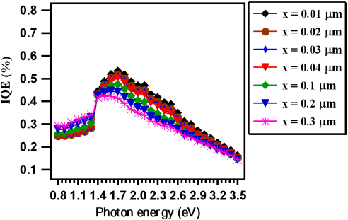
Figure 4. Influence of the Cu2O buffer layer thickness on the internal quantum efficiency: case of the solar cell with TiO2 window layer.
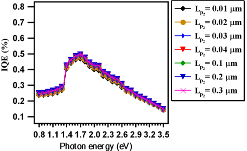
Figure 5. Evolution of the internal quantum efficiency with the minority carrier diffusion lengths in the Cu2O buffer layer: case of the solar cell with the TiO2 window layer.
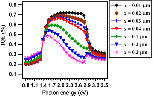
Figure 6. Influence of the Cu2O buffer layer thickness on the internal quantum efficiency: case of the solar cell with ZnO window layer.
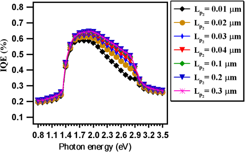
Figure 7. Evolution of the internal quantum efficiency with the minority carrier diffusion lengths in the Cu2O buffer layer: case of the solar cell with the SnO2 window layer.
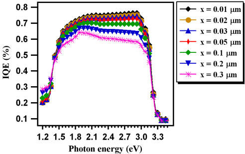
Figure 8. Influence of the NiO buffer layer thickness on the internal quantum efficiency: case of the solar cell with ZnO window layer.
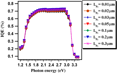
Figure 9. Evolution of the internal quantum efficiency with the minority carrier diffusion lengths in the NiO buffer layer: case of the solar cell with the ZnO window layer.
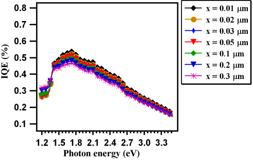
Figure 10. Influence of the NiO buffer layer thickness on the internal quantum efficiency: case of the solar cell with TiO2 window layer.
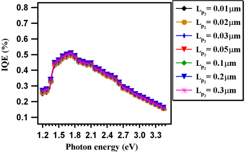
Figure 11. Evolution of the internal quantum efficiency with the minority carrier diffusion lengths in the NiO buffer layer: case of the solar cell with the TiO2 window layer.
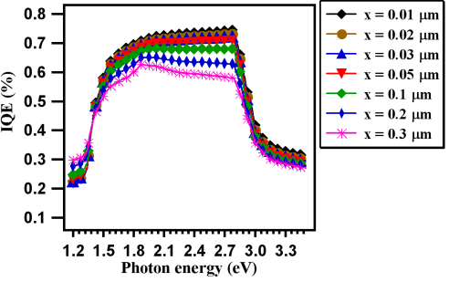
Figure 12. Influence of the NiO buffer layer thickness on the internal quantum efficiency: case of the solar cell with SnO2 window layer.
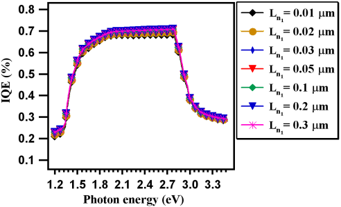
Figure 13. Evolution of the internal quantum efficiency with the minority carrier diffusion lengths in the NiO buffer layer: case of the solar cell with the SnO2 window layer.
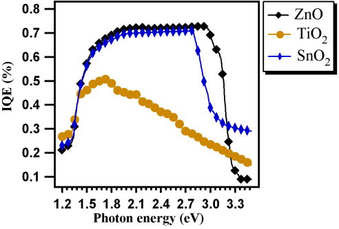
Figure 14. Internal quantum efficiency as a function of photon energy for the three models: ZnO(n+)/NiO(n)/CH3NH3Sn0.75Ge0.25I3(p), TiO2(n+)/NiO(n)/CH3NH3Sn0.75Ge0.25I3(p) and SnO2(n+)/NiO(n)/CH3NH3Sn0.75Ge0.25I3(p).